Base fee for PCBA set up.
This includes the stencils, packaging etc.
The cost of soldering the components onto the boards.
This is the price of your components, spare parts and the cost in procurement.
This includes handling fee and sales margin, etc.
This includes fees for certification, mechanical parts and other requirements as specified. Requires manual quotation.
Production time is the period between file confirmation to packing. Another day is required for dispatch. File review and subsequent delays caused by problems in the files is not included.
Learn MoreFR-4 is the most commonly used material for PCBs. One sided aluminum boards have traces on one side and bare aluminium on the other. They are good for heat dissipation. For multi-layer aluminium PCBs please use the Advanced service. Flexible Printed Circuit boards (FPC) are much thinner than FR-4 and can be bent to some extent.
Learn MoreThe number of circuit layers in your boards. If you choose 1 layer, then the non-circuit side will not be covered with solder mask.
Learn MoreUp to 600mm*800mm, if you panelize the board, please fill the dimension of panel.
The number of boards/panels required. If your files are of a single board then this is the number of boards. If your boards are panelised into a panel, then this is the number of panels.
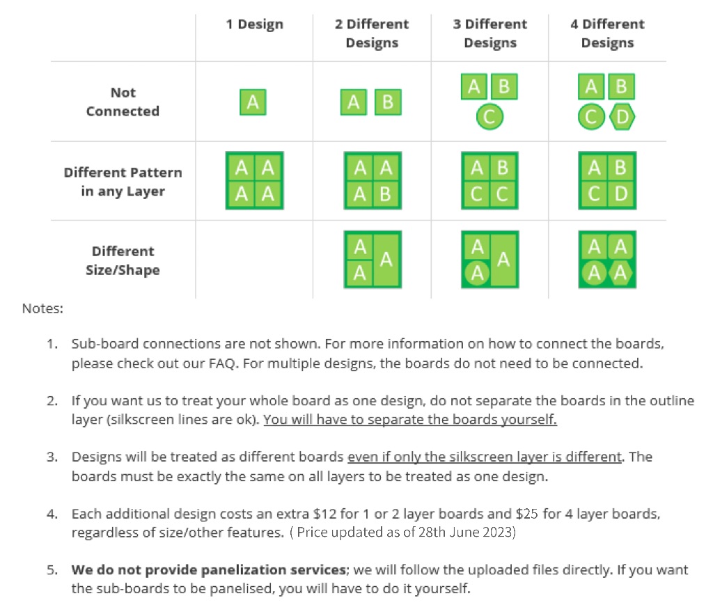
Learn MoreHow many different designs in your files separated by v-cuts, stamp holes or milling slots. Please see the example. Different designs are not accepted for multi-layer boards with over 6 circuit layers. Seeed does not provide panelisation services, if you want panelised boards, please design the panelised Gerber data yourself.
Learn MoreThe final thickness of the finished PCBs. Board thickness tolerance is +/-10%. Solder mask and copper plating may make the boards slightly thicker.
Learn MoreThe color of the solder mask applied onto the base material. For most colors, the silkscreen is printed white. Only for white solder mask, the silkscreen is printed black. No mixing of solder mask colors is allowed. Green solder mask has the best performance.
Learn MoreHASL (Hot Air Solder Level) processing applies a thin layer of solder on the pads. ENIG (Electroless Nickel/Immersion Gold) has better planarity and shelf life than HASL and is lead free. Hard gold is useful for gold fingers. Choosing this option, the entire board will be plated in Hard Gold. For ENIG + Hard Gold please use the Advanced service.
Learn MoreCopper weight on the outer layers (top and bottom). The copper weight for inner layers is fixed at 0.5oz. If you need other weights please contact us directly or use the Advanced service.
Learn MoreThe minimum drill hole size required in the PCB. Drill hole sizes under 0.3mm are much more difficult to produce. For batch production please ensure hole size is more than 0.3mm.
Learn MoreThe minimum width of the traces and the minimum space between traces in your design. If your design needs to be batch produced, please ensure that the width and spacing is greater than 6 mil.
Learn MoreWhether or not your boards require plated half-holes/castellated holes. These are holes on the edge of the board that require copper plating. This is a specialised process, we cannot v-cut or mill plated holes.
Learn MoreWhether or not traces on the board need to meet impedance requirements. Please include impedance documentation in your upload. For more complex requirements, we may contact you for extra fees.
Learn MoreVias are filled with non-conductive epoxy then capped with pads on both sides. Essential for BGA via-in-pads to prevent solder leakage during assembly.
Follow the quality standard